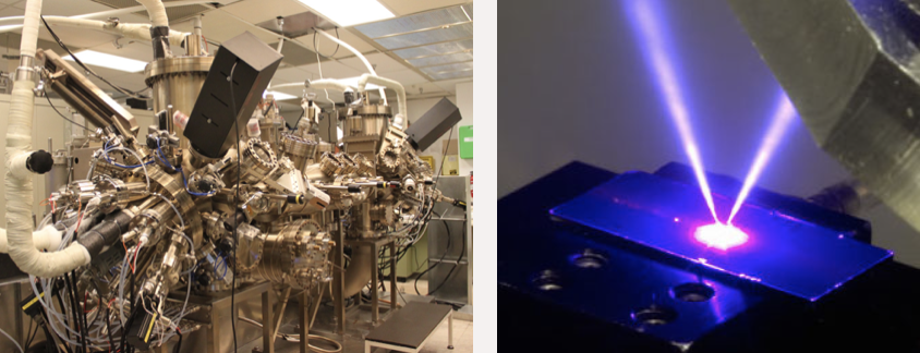
MBE growth of various kinds of III-V and II-VI compound semiconductors.
A unique twin-chamber MBE system allows growth of any composition of III-V and II-VI alloys. Monolithic intergration material platform for various optoelectronic and electronic device applications.
- he II-VI chamber is capable of growing almost all possible combinations of materials including Zn, Se, Te, Mg, Be, and Cd. The Se and Te cells are valved cell to allow for precise control of composition and graded layers. In addition, it contains five different dopants (Al, Ga, P, Bi, and In) so that various doping profiles in different material systems can be studied.
- The III-V chamber contains various group III and V cells including Ga, In, Al, As, Sb and P, which can cover all the typical III-V combinations. The new Bi cell enhances our growth capability to bismide materials. The specially designed doping cell, which contains Be, Te and Si, can satisfy different doping requirements.
S. Wang et al., J. of Cryst. Growth 311, 2116-2119 (2009).
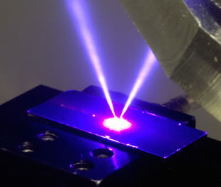
II–VI materials lattice matched to GaSb substrates are desirable for ultrahigh-efficiency multijunction solar cells. We report growth of ZnTe and ZnCdTe/ZnTe quantum wells on undoped GaSb (1 0 0) substrates using MBE. Post-growth structural characterization using X-ray diffraction and high-resolution transmission electron microscopy reveals very low-defect density, i.e. high crystalline quality. Visible photoluminescence is observed from 10 to 300 K.
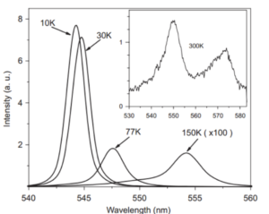 PL from a ZnCdTe/ZnTe quantum well at different temperatures, with 300 K data shown in inset.
J. Fan, et al., J. of Cryst. Growth 323, 127-131 (2010).
Thick ZnTe grown on III–V substrates is proposed as a low-cost virtual substrate for electronic and optoelectronic device applications based on 6.1 Å compound semiconductors. This paper reports the growth of ZnTe samples on GaAs, InP, InAs and GaSb (0 0 1) substrates using MBE. XRD analysis indicates there are residual tensile strains in ZnTe epilayers due to the difference in thermal expansion coefficients between the ZnTe epilayers and the different substrate materials. HREM images reveal the presence of Lomer edge and 60° partial dislocations at the interfaces between ZnTe epilayers and GaAs and InP substrates. Visible photoluminescence from ZnTe epilayers is observed from 80 to 300 K.
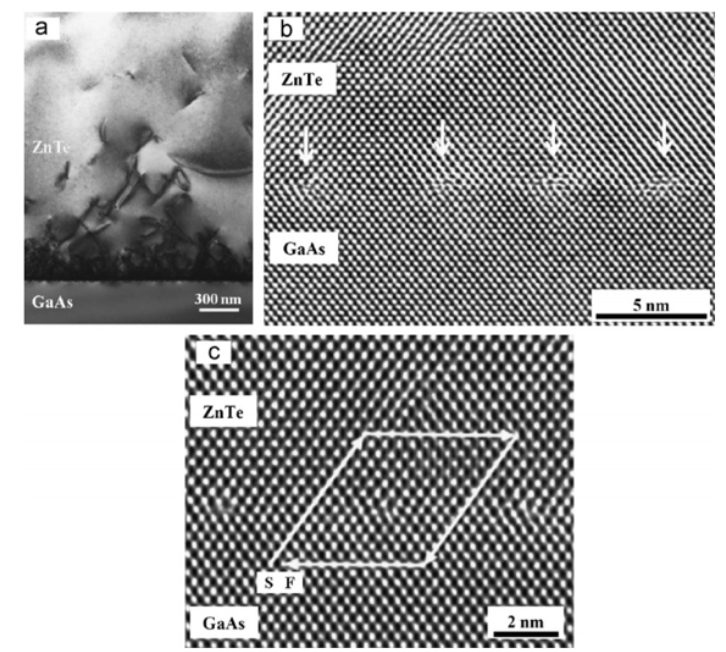
(a) Low magnification HREM image of ZnTe/GaAs (0 0 1) sample. (b) High magnification HREM image. (c) High-resolution image showing ZnTe/GaAs interface with Burgers’ circuit. S and F indicate the start and finish points for the Burgers’ circuit analysis.
J. Fan, et al., Applied Physics Letters 101 (12), 121909 (2012).
ZnTe/GaSb distributed Bragg reflectors (DBRs) are proposed and demonstrated for mid-wave infrared (2–5 µm) optoelectronic applications. A series of ZnTe/GaSb DBR structures have been successfully grown on GaSb (001) substrates using molecular beam epitaxy. X-ray diffraction results reveal smooth interfaces, uniform thicknesses, and low defect density. The DBR sample of seven k/4 pairs has a peak reflectance as high as 99.0% centered at 2.5 µm with a 480-nm wide stopband.
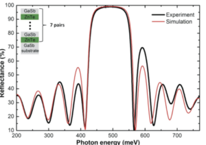
Measured and simulated reflectance spectra for a ZnTe/GaSb DBR sample of seven k/4 pairs.
M. J. DiNezza, et al., physica status solidi (c), 9, 1720–1723 (2012).
ZnTe PN homojunctions are fabricated using thermal diffusion of Al into a ZnTe film grown on lattice-matched GaSb substrates by molecular beam epitaxy. Rectifying J-V characteristics and the photovoltaic effect are observed which suggests that n-type ZnTe has been successfully achieved. Photoluminescence measurements of annealed ZnTe samples without the Al diffusion layer show strong band-edge luminescence at room temperature. This technique may lead to a better understanding of the n-type doping problem for ZnTe, and could lead to in-situ doping techniques and treatments.
J. Fan, L., et al., J. Vac. Sci. Technol. B, 30, 02B122 (2012).
This paper reports high-quality GaSb grown on ZnTe using molecular beam epitaxy with a temperature ramp during growth. During growth, in situ RHEED shows rapid and smooth transition from ZnTe surface reconstruction to GaSb surface reconstruction. Post-growth structural characterization using x-ray diffraction and transmission electron microscopy reveals smooth interface morphology and low defect density. Strong photoluminescence emission is observed up to 200 K. The sample grown with a temperature ramp from 360 to 470 °C at a rate of 33 °C /min showed the narrowest bound exciton emission peak with a full width at half maximum of 15 meV.
J. Fan, et al., J. of Crystal Growth 371 (1), 122–125 (2013).
A series of GaSb/ZnTe double-heterostructures proposed for laser diode applications was successfully grown by molecular beam epitaxy using GaSb (001) substrates. Post-growth characterization using high-resolution X-ray diffraction and transmission electron microscopy reveals low defect density and coherent interface morphology. Strong photoluminescence emission is observed at temperatures up to 200 K, indicating good optical properties.
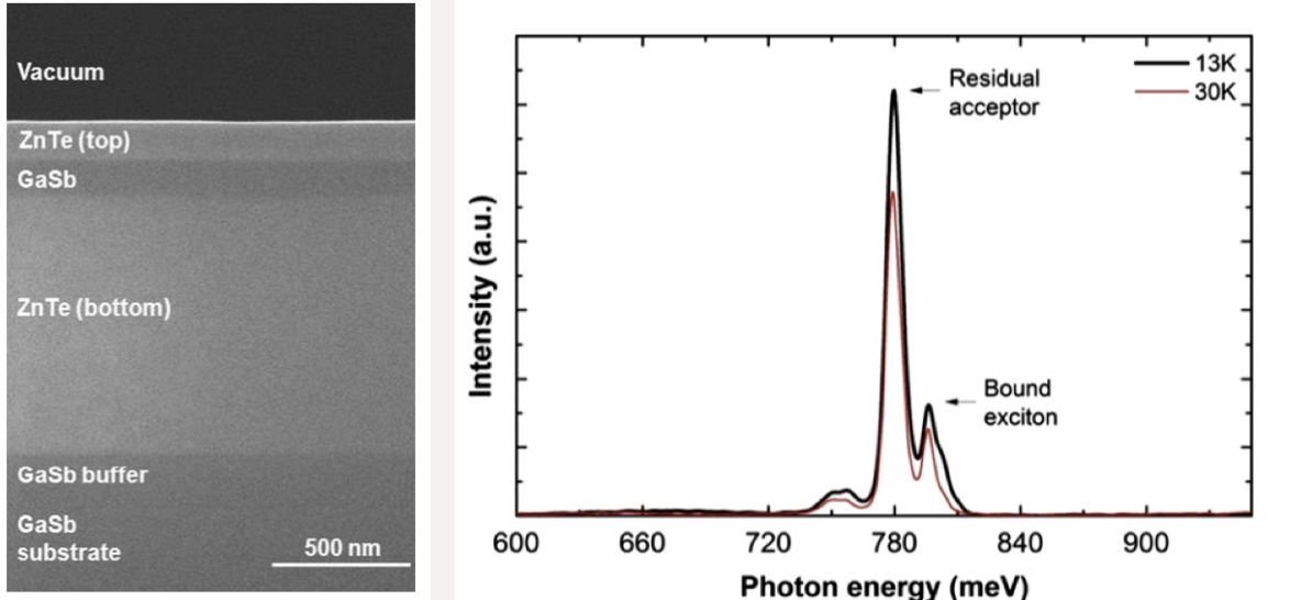
SEM image showing cross-section of GaSb/ZnTe DH sample and PL spectra for GaSb/ZnTe DH
sample measured with excitation density of 10 W/cm2 at 13 K (in black), and 30 K (in red).
H. Li, S. et al, J. of Crystal Growth 378, 145-149 (2013).
A calibration method for group V fluxes is demonstrated for the growth of InAsxSb1−xalloys and strain-balanced InAs/InAsxSb1−x superlattices on GaSb substrates by MBE for IR optoelectronic device applications. Samples grown at 450 °C with Sb/In flux ratios from 1.0 to 2.0 and As/In flux ratios from 1.2 to 2.5 lead to Sb mole fractions ranging from 0.078 to 0.34. High structural and optical quality superlattices for Sb mole fractions up to 0.34 are verified by XRD and low-temperature PL measurements. When varying both Sb mole fraction and period, superlattice structures are demonstrated with low-temperature emission wavelengths ranging from 3.6 to 7.1 μm.
S. Liu, et al., Appl. Phys. Lett. 102, 071903-071903-4 (2013).
Molecular beam epitaxial growth of strain-balanced InAs/InAs1xSbx type-II superlattices on GaSb substrates has been investigated for substrate temperatures from 400°C to 450° C. The Sb composition is found to vary linearly with substrate temperature at constant V/III ratios. For samples grown at the optimized substrate temperature (410 °C), superlattice zero-order peak full-width at half-maximums are routinely less than 25 arc sec using high-resolution X-ray diffraction.
J. Fan, et al., J. Vac. Sci. Technol. B 31, 03C109 (2013).
This paper reports the molecular beam epitaxial growth and characterization of high-reflectivity and broad-bandwidth distributed Bragg reflectors (DBRs) made of ZnTe/GaSb quarter-wavelength (λ/4) layers for optoelectronic applications in the midwave infrared spectral range (2-5 µm). Post-growth characterization using high-resolution x-ray diffraction, atomic force microscopy, and transmission electron microscopy reveals smooth surface morphology, low defect density, and coherent interfaces. Reflectance spectroscopy results show that a DBR sample of seven λ/4 pairs has a peak reflectance as high as 99.0% centered at 2.56 µm with a bandwidth of 517 nm.
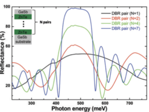
Experimental reflectance spectra for the ZnTe/GaSb DBR samples with different number of k/4 pairs (N= 1, 2, 4, 7).