Type-II Superlattice Semiconductors for Infrared Photodetectors
E. H. Steenbergen, et al., Appl. Phys. Lett. 99, 251110 (2011).
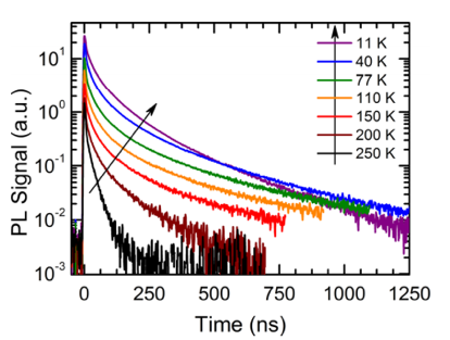
Time-resolved photoluminescence measurements reveal a minority carrier lifetime of >412 ns at 77 K under low excitation for a long-wavelength infrared InAs/InAs0.72Sb0.28 type-II superlattice (T2SL). The considerably longer lifetime is attributed to a reduction of non-radiative recombination centers with the removal of Ga from the superlattice structure. This lifetime improvement may enableT2SL long-wavelength infrared photodetectors at higher operating temperatures.
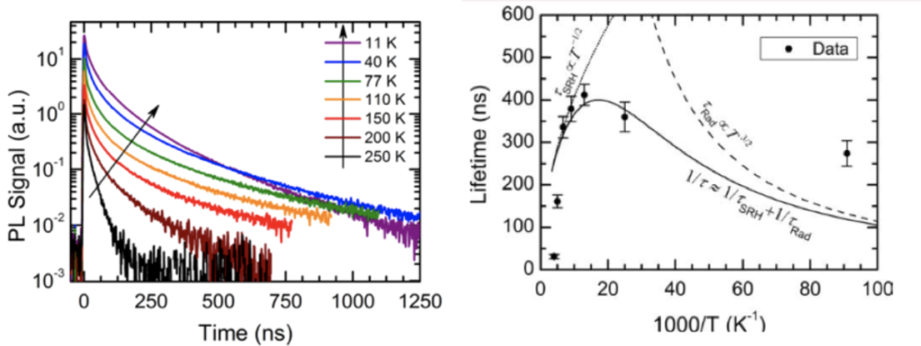
(a).Combined temperature-dependent time-resolved photoluminescence decay measurements. (b). Carrier lifetimes extracted from the previous figure. Also plotted is the temperature dependence of the SRH lifetime (τSRH ∝ T −1/2), radiative lifetime (τRad ∝ T 3/2), and a combination of both SRH and radiative lifetimes (solid line).
E. H. Steenbergen, et al., Appl. Phys. Lett. 99, 071111 – 071114 (2011).
Strain-balanced type-II InAs/InAs1–xSbx superlattices with various compositions (x¼ 0.22, 0.23, 0.37) and different layer thicknesses (tInAs= 7 nm, tInAsSb= 3.3, 2.3, 2.0 nm, respectively) have been grown by metalorganic chemical vapor deposition on GaSb substrates. X-ray diffraction revealed narrow satellite peaks (full-width-half-maximum of 100 arc sec), indicative of uniform superlattice periodicity and excellent crystallinity, which was also corroborated by cross-sectional transmission electron microscopy observations.
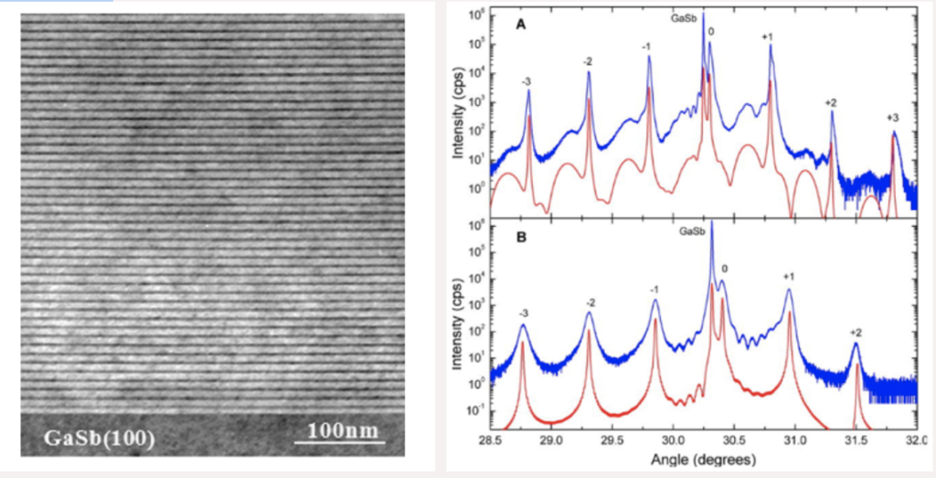
(a).Cross-sectional transmission electron micrograph of sample A demonstrating the excellent crystallinity of the InAs/InAsSb superlattice grown on a GaSb (100) substrate. (b).High-resolution (004) XRD patterns and simulations (offset below each measurement) for samples A and B.
H.S. Kim, et al., Applied Physics Letters 101, 161114 (2012).
Long-wave infrared InAs/InAsSb type-II superlattice nBn photodetectors are demonstrated on GaSb substrates. The typical device consists of a 2.2 µm thick absorber layer and has a 50% cutoff wavelength of 13.2 µm, a measured dark current density of 5 104 A/cm2 at 77 K under a bias of 0.3 V, a peak responsivity of 0.24 A/W at 12 µm, and a maximum resistance-area product of 300 X cm2 at 77 K. The calculated generation-recombination noise limited specific detectivity (D*) and experimentally measured D* at 12 µm and 77 K are 1 x 1010 cm Hz1/2/W and 1 108 cm Hz1/2/W, respectively.
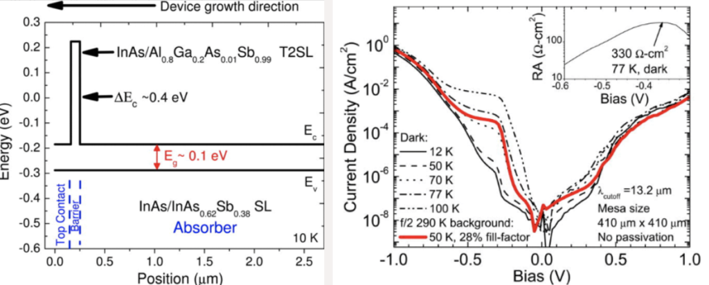
(a). Designed energy band diagram of T2SL nBn photodetector using the three-band Kronig-Penney model calculation. The conduction band offset between the barrier and the absorber is ∼0.4 eV. (b). Dark current density as a function of applied bias ranging from 12 K to 100 K, the solid color line shows the total current under 290 K background with f/2 optics at 50 K with 28% optical aperture fill-factor. The inset shows dynamic dark RA product at 77 K.
E. H. Steenbergen, et al., J. Vac. Sci. Technol. B 30, 02B107 (2012);
Strain-balanced InAs/InAs1−xSbx type-II superlattices (SLs) on GaSb substrates with 0.27 ≤ x ≤0.33 were grown by molecular beam epitaxy and demonstrated photoluminescence (PL) up to 11.1 μm. X-ray diffraction measurements reveal average SL mismatches of less than 0.2%, and the PL full-width-at-half-maximums increase with the mismatch.
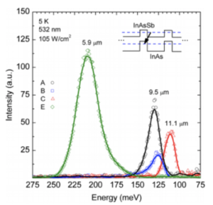
Photoluminescence spectra at 5 K for InAs/ InAs1xSbx type-II superlattice samples A, B, C, and E with varying compositions and periods. The inset shows a schematic of the SL band alignment and PL transition.
H. Li, S. et al, J. of Crystal Growth 378, 145-149 (2013).
A calibration method for group V fluxes is demonstrated for the growth of InAsxSb1−x alloys and strain-balanced InAs/InAsxSb1−x superlattices on GaSb substrates by MBE for IR optoelectronic device applications. Samples grown at 450 °C with Sb/In flux ratios from 1.0 to 2.0 and As/In flux ratios from 1.2 to 2.5 lead to Sb mole fractions ranging from 0.078 to 0.34. High structural and optical quality superlattices for Sb mole fractions up to 0.34 are verified by XRD and low-temperature PL measurements. When varying both Sb mole fraction and period, superlattice structures are demonstrated with low-temperature emission wavelengths ranging from 3.6 to 7.1 μm.
S. Liu, et al., Appl. Phys. Lett. 102, 071903-071903-4 (2013).
Molecular beam epitaxial growth of strain-balanced InAs/InAs1-xSbx type-II superlattices on GaSb substrates has been investigated for substrate temperatures from 400°C to 450° C. The Sb composition is found to vary linearly with substrate temperature at constant V/III ratios. For samples grown at the optimized substrate temperature (410 °C), superlattice zero-order peak full-width at half-maximums are routinely less than 25 arc sec using high-resolution X-ray diffraction.
X.-M. Shen, et al., J. of Cryst. Growth 381, 1-5 (2013).
InAs/InAs1−xSbx type-II superlattices (SLs) have been grown on GaSb (100) substrates using molecular beam epitaxy with different Sb/In and As/In flux ratios and growth temperatures ranging from 400 °C to 450 °C. High-resolution x-ray diffraction reveals increase in Sb composition as either growth temperature or the ratio of As/Sb is decreased. Cross-sectional electron micrographs show excellent crystallinity, particularly for those samples grown close to the strain-balanced condition at lower temperatures and those with higher Sb/As flux ratios.
X.-M. Shen, et al., Bulletin of the American Physical Society (2015).
The zero valence-band offset between the barrier and absorber of a nBn photodetector is challenging to achieve practically, which could lead to different electrical characteristics. Long-wave (Sample A) and mid-wave (Sample B) infrared nBn photodetectors with absorbers consisting of InAs/InAsSb SLs and barriers consisting of InAs/AlGaSb(As) SLs, were grown using MBE. Examination of the barrier layers using off-axis electron holography showed the presence of positive charge with an estimated density of 1.8 x 1017cm 3 in Sample B as a result of a type-II band alignment, whereas negligible charge was detected in Sample A, consistent with a type-I band alignment. This staggered type-II alignment of Sample B caused the significant increase in its dark current when strong bias is applied, because electrons from the valence band of the barrier layer can tunnel to the conduction band of the absorber layer.
Z.-Y. Lin, et al., Appl. Phys. Letters 107, 201107 (2015).
A long minority carrier lifetime of 12.8 μs in a mid-wavelength infrared InAs/InAsSb type-II superlattice is observed at 15 K using time-resolved photoluminescence technique. The long carrier lifetime is due to carrier localization, which is confirmed by a 3 meV blue shift of the photoluminescence peak energy and the monotonic decrease of lifetime with increasing temperature from 15 K to 50 K, along with an increased photoluminescence linewidth below 40 K. In contrast, no carrier localization is observed in a long-wavelength infrared type-II superlattice at the same temperatures. Modeling results show that carrier localization is stronger in shorter period (9.9 nm) mid-wavelength infrared superlattices as compared to longer period (24.2 nm) long-wavelength infrared superlattices, indicating that the carrier localization originates mainly from InAs/InAsSb interface disorder.
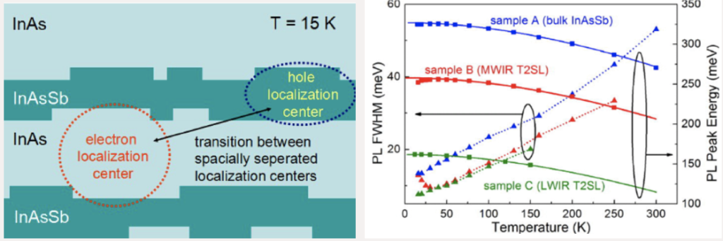
(a). Figure demonstrating carrier localization in a type-2 superlattice. (b). Photoluminescence (PL) peak energy and full-width at half maximum (FWHM) of samples A (bulk InAsSb), B (MWIR InAs/InAsSb T2SL), and C (LWIR InAs/InAsSb T2SL) as a function of temperature. As temperature increases from 15 K to 50 K, the peak energy of sample B increases by 3 meV and the FWHM decreases by 3 meV, indicating carrier localization. The solid lines show the Varshni fit of PL peak energy as a function of temperature.
X.-M. Shen, et al., Appl. Phys. Letters 107, 122109 (2015).
Mid-wave and long-wave infrared nBn photodetectors with absorbers consisting of InAs/InAsSb superlattices and barriers consisting of InAs/AlGaSb(As) superlattices were grown using molecular beam epitaxy. High-resolution X-ray diffraction showing significant differences in Ga composition in the barrier layer, and different dark current behavior at 77 K, suggested the possibility of different types of band alignments between the barrier layer and the absorber for the mid- and long-wave infrared samples.