The MBE laboratory is equipped with four solid source MBE chambers for growing III-V and II-VI semiconductor materials. All chambers are equipped for reflection high energy electron diffraction (RHEED) characterization and are fully computer controlled.
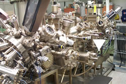
VG V80H (Chamber A and B)
The group’s oldest system is a VGV80H twin-chamber MBE system. Chamber A is dedicated to the growth of II-VI compound semiconductors such as ZnTe, CdTe, and CdSe. Chamber B is dedicated to the growth of III-V compound semiconductors such GaAs, InP, GaSb, and InAs. Ths MBE system enable us to grow various optoelectronic devices (solar cells, laser diodes, light emitting diodes, optical refrigeration devices, photodetectors, and photovaltic devices) for wavelengths ranging from 300 nm to 3 mircrons.
Sources
Chamber A: Zn, Cd, Te, Se, Bi, N, GaP, Al
Chamber B: Ga, Al, In, As, Sb, P, Be, Si, Te, CBr4
VG V80H (Chamber C and D)
The group recently obtained another V80H MBE system which will be used to grow II-VI and III-V compounds in the same chamber. This unique setup gives the group the ability to grow heterovalent structures that have never been realized with MBE. In addition to traditional solid-source effusion cells, chamber C will also be equipped with an e-beam system for refractory metal deposition. Chamber C will be brought online in the near future, with chamber D following later.
Sources
Chamber C: Zn, Ga, As, Sb, Bi, Se, Te, Mo, Nb, Fe, Co
Chamber D: TBD
For more info on MBE, please see these three videos (1, 2, 3) of lectures given by epitaxy pioneers at the 2014 International Conference on Molecular Beam Epitaxy.
NOTICE: All equipment is available to external users at reasonable cost. Please contact us for further details.