by Fulton Schools | Jan 31, 2018
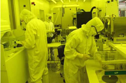
Semiconductor device processing is carried out in a 4,000 square foot class-100 cleanroom in the ASU NanoFab facility. List of major equipments and systems Tempress 8-stack furnace tubes configured for: wet and dry thermal oxidation; poly-silicon, low temperature...