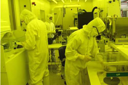
Semiconductor device processing is carried out in a 4,000 square foot class-100 cleanroom in the ASU NanoFab facility.
List of major equipments and systems
- Tempress 8-stack furnace tubes configured for: wet and dry thermal oxidation; poly-silicon, low temperature oxide and silicon nitride CVD; phosphorus and boron doping; and the annealing of 4” silicon wafers.
- Heidelberg DWL 66 Mask Making and Optical Direct-Write
- Karl Suss MJB3 Contact Aligner
- EVG 620 Front and Backside Aligner
- JEOL JBX-6000FS/E Electron Beam Lithography System
- Sloan/Varian 841 Electron Beam Evaporator
- Torrvac VC-320 Electron Beam Evaporator
- CHA 600-SE Electron Beam Evaporator
- CHA 1000-SE E-beam Evaporator
- Edwards Auto306 Thermal Evaporator
- MRC-8617 RF Sputter Coater
- Woollam Ellipsometer WVASE32
- Rudolph AutoEL II Ellipsometer
- Dektak IIA Profilometer
- Filmetrics F20
- Hitachi S4700 Field Emission Scanning Electron Microscope with Energy Dispersive x-ray Analysis
- PlasmaQuest 333 RPCVD
- Tamarack 180M
- Heat Pulse 610 RTP
- Jipelec
- STS ICP Advanced Silicon Etch (ASE)
- STS ICP All General Etch (AGE)
- PlasmaLab µ P80 Reactive Ion Etcher
- Tegal PlasmaLine 411 Plasma Asher
- EVG620 Mask Aligner
- EVG520HE Bonder and Semi-automated Hot Embossing
NOTICE: All equipment is available to external users at reasonable cost. Please contact us for further details.


